Showing posts with label DC. Show all posts

Saturday, December 21, 2013

High & Low voltage cut-off with delay& alarm

High & Low voltage cut-off with delay& alarm

Description.
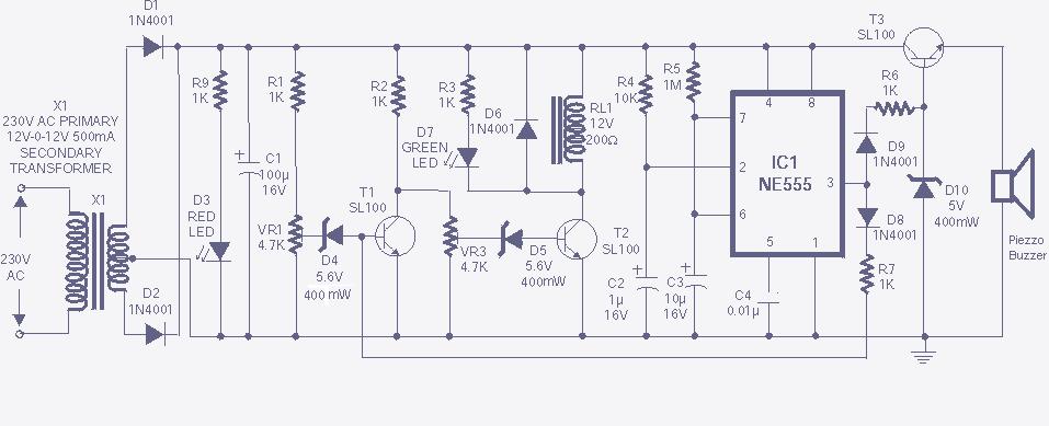
This straight forward circuit will protect electrical appliances from over voltage as well as under voltage. The circuit also produces an alarm when the power supply comes back. An ideal circuit for home to protect your valuable equipments from voltage fluctuations. The same circuit with some modifications can be used  to make a automatic voltage stabilizer.
When the mains voltage is in the normal level, the voltage at the negative terminal of zener diode D4 will be less than 5.6 Volts. At this condition transistor T1 will not conduct. The same time voltage at the negative terminal of zener diode D5 will be greater than 5.6 and so the transistor T2 will be conducting. The relay will be activated and the green LED will be glowing.
When the mains voltage is higher than the set limit the transistor T1 becomes conducting since the voltage at the negative terminal of  D4 is greater than 5.6 V. At the same time transistor T2 will be non conducting which results in the deactivation of relay to cut the mains supply from load. When the mains voltage is less than the set limit transistors T1 & T2 becomes non conducting  making the relay to de-activate and cut the load from mains.
The timer NE555 is wired as a monostable multivibrator with a pulse width of 10ms.When the power comes back after a cut off a negative voltage is obtained at the trigger pin which triggers the IC NE555. The transistor T3 gets forward biased and it drives the buzzer to produce a beep as an indication of power resumption. Also the transistor T1 is made on which in turn makes T2 off. As a result the relay will remain de- activate for 10ms and this provides the sufficient delay and the equipment  is protected from surge voltages.
Circuit diagram with Parts list.Click to enlarge.
high-and-low-voltage-cut-of-circuit
Notes.
  • To calibrate the circuit a autotransformer is needed. Connect the output of autotransformer to the transformer primary.
  • Set the voltage to 260V and adjust  VR1 to make the relay deactivated.
  • Now set the autotransformer to 160V and adjust VR2  so that the relay is de-energized.
  • VR3 can be used to vary the volume of buzzer.

Friday, December 20, 2013

Voltage Multiplier

Voltage Multiplier

                                We require high voltage at certain applications ,we see mosquito bats to kill mosquito , in that we produce a high voltage from a battery . we can use this circuit for making high voltage from a low voltage source         
This circuit produces a very high voltage and care must be used to prevent getting a nasty shock.  The transformer can produce over 1,000v and the 8-stage multiplier can produce up to 20,000v 
.


circuit diagram

555 Timer as Monostable Multivibrator

555 Timer as Monostable Multivibrator


A monostable multivibrator (MMV) often called a one-shot multivibrator, is a pulse generator circuit in which the duration of the pulse is determined by the R-C network,connected externally to the 555 timer. In such a vibrator, one state of output is stable while the other is quasi-stable (unstable). For auto-triggering of output from quasi-stable state to stable state energy is stored by an externally connected capaci­tor C to a reference level. The time taken in storage determines the pulse width. The transition of output from stable state to quasi-stable state is accom­plished by external triggering. The schematic of a 555 timer in monostable mode of operation is shown in figure. 

555-timer-monostable-multivibrator
Pin 1 is grounded. Trigger input is applied to pin 2. In quiescent condition of output this input is kept at + VCC. To obtain transition of output from stable state to quasi-stable state, a negative-going pulse of narrow width (a width smaller than expected pulse width of output waveform) and amplitude of greater than + 2/3 VCC is applied to pin 2. Output is taken from pin 3. Pin 4 is usually connected to + VCC to avoid accidental reset. Pin 5 is grounded through a 0.01 u F capacitor to avoid noise problem. Pin 6 (threshold) is shorted to pin 7. A resistor RA is connected between pins 6 and 8. At pins 7 a discharge capacitor is connected while pin 8 is connected to supply VCC.


555 IC Monostable Multivibrator Operation.

http://www.circuitstoday.com/wp-content/uploads/2009/09/monostable-multivibrator-operation.jpg


555 monostable-multivibrator-operation

For explain­ing the operation of timer 555 as a monostable multivibrator, necessary in­ternal circuitry with external connections are shown in figure.
The operation of the circuit is ex­plained below:

Initially, when the output at pin 3 is low i.e. the circuit is in a stable state, the transistor is on and capacitor- C is shorted to ground. When a negative pulse is applied to pin 2, the trigger input falls below +1/3 VCC, the output of comparator goes high which resets the flip-flop and consequently the transistor turns off and the output at pin 3 goes high. This is the transition of the output from stable to quasi-stable state, as shown in figure. As the discharge transistor is cut­off, the capacitor C begins charging toward +VCC through resistance RA with a time constant equal to RAC. When the increasing capacitor voltage becomes slightly greater than +2/3 VCC, the output of comparator 1 goes high, which sets the flip-flop. The transistor goes to saturation, thereby discharging the capacitor C and the output of the timer goes low, as illustrated in figure.

Thus the output returns back to stable state from quasi-stable state.

The output of the Monostable Multivibrator remains low until a trigger pulse is again applied. Then the cycle repeats. Trigger input, output voltage and capacitor voltage waveforms are shown in figure.
Monostable Multivibrator Design Using 555 timer IC

The capacitor C has to charge through resistance RA. The larger the time constant RAC, the longer it takes for the capacitor voltage to reach +2/3VCC.

In other words, the RC time constant controls the width of the output pulse. The time during which the timer output remains high is given as

tp = 1.0986 RAC
where RA is in ohms and C is in farads. The above relation is derived as below. Voltage across the capacitor at any instant during charging period is given as

vc = VCC (1- e-t/RAC)

Substituting vc = 2/3 VCC in above equation we get the time taken by the capacitor to charge from 0 to +2/3VCC.

So +2/3VCC. = VCC. (1 – e-t/RAC) or t – RAC loge 3 = 1.0986 RAC

So pulse width, tP = 1.0986 RAC s 1.1 RAC

The pulse width of the circuit may range from micro-seconds to many seconds. This circuit is widely used in industry for many different timing applications.

555 DC to AC inverter circuit diagram

555 DC to AC inverter circuit diagram


This is inverter circuit diagram.Here I have used famous Transistors TIP41 and TIP42.And the frequency is generated by NE555.By using R4 you can control the frequency.out put voltage is 120V-230V.the frequency is 50Hz.This circuit operates with 5V-15V.


Note

# Be careful because you are dealing with 230V.

#This circuit is not suitable for kids.

#Use heat sinks for transistors