Saturday, December 21, 2013

The story of Fibonacci series

The story of Fibonacci series

All of you must have heard about the term “Fibonacci series”. Many of you (including me) might have written programs in different programming languages to generate a “Fibonacci series”. It is quite interesting to see that tutorials of all programming languages would contain a problem to generate fibonacci series upto “N” terms.  Well, this made me a little curious. What is so important with this particular series? In mathematics, there may be a 100 or 1000 types of series – but why “Fibonacci” is learned by everyone?
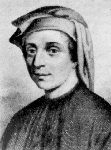
Leonardo of Pisa
Now let’s get into the story. Fibonacci series is – 0,1,1,2,3,5,8,13,21,34,55,89,144,233,377… it moves to infinity. This series is named after the famous Italian mathematician - Leonardo of Pisa (aka Fibonacci). His period of life is assumed to be in between 1175 AD to 1250 AD.  Leonardo’s father was a merchant in the port of Pisa. As a young boy, Leonardo traveled extensively with his father across the mediterranean sea shores. The Mediterranean sea  (known in latin as “middle of land”) connects together 3 continents – Africa, Europe and Asia. Trade had been happening between major ports of all these continents and Leonardo actively involved in these trades with his father. Leonardo and his people who belonged to Europe, was using Roman numerals for trade calculations. The Europeans were completely unaware of the “Hindu Arabic” system which was used by Arab traders in Asian/African countries (this is the presently known decimal number system ). The basic difference between a Roman numeral system and “Hindu Arabic system” is shown below. 
Roman Numerals  has no symbol for zero. They dont have a symbol for 2,3,4,7,8 and 9. Instead they were depending upon the symbols for 1,5,10,50,100,500 and 1000 for their calculations.  See the table below. 
I
1
V
5
X
10
L
50
C
100
D
500
M
1000
So to represent 1910 – Romans would write – MDCCCCX. The interesting thing is you can write this in any order – means – CCCCDMX – would also read 1910. This is because the number is read finally by calculating M+D+C+C+C+C+X. It was very difficult to add or subtract two numbers using the roman number system. If you are interested in knowing how calculations are performed in roman system – follow this link – Roman numeral calculations.
The “Hindu Arabic” system was quiet different. They only had symbols for numbers from 0 to 9. This is our decimal number system. Higher numbers were represented in this system by repeated addition or repeated subtraction. This means 1910 in “Hindu Arabic” is  1000 one times + 100 nine times + 10 one time + 1 zero times. 
Note: History says that this system originated in India. Arabs learned this from Indians (as part of their Eastern trade) and they called this “Hindu Numerals”. Later westerns learned this from Arabs and they called this system “Arab Numerals”
Leonardo learned about various methods used by merchants for calculations and he found the “Hindu-Arabic” system very easy and convenient to perform mathematical calculations compared to the cumbersome “Roman numerals” method. He later introduced this “Hindu Arabic” system in Europe and he documented the system and how to make calculations using this system in a book called “Liber Abaci” (1202 AD). This “new” system later influenced many European mathematicians. 

The Fibonacci series… 

This series is invented by Leonardo in an attempt to solve a real life problem. A rabbit farmer wanted to know how many rabbits he can grew in a year from one pair. The problem is quiet an interesting one. A pair of rabbits bear another new pair in a single month. This new born pairs can bear another pair after the first month. 
Now he explains the problem as:- 
Because the above written pair in the first month bore, you will double it; there will be two pairs in one month.
One of these, namely the first, bears in the second montth, and thus there are in the second month 3 pairs;
of these in one month two are pregnant and in the third month 2 pairs of rabbits are born, and thus there are 5 pairs in the month;

there will be 144 pairs in this [the tenth] month;
to these are added again the 89 pairs that are born in the eleventh month; there will be 233 pairs in this month.
To these are still added the 144 pairs that are born in the last month; there will be 377 pairs, and this many pairs are produced from the abovewritten pair in the mentioned place at the end of the one year.
So that is the real origin of Fibonacci series. This series is invented in an attempt to solve a real life business problem of – “how many rabbits can be made from a single pair in an year” .  
I said, “business problem” because Leonardo  was basically involved in trade and this problem of rabbits might have raised to him by one of his business contact! 

Other interesting facts:- 

After the eighth sequence of calculations, there are constant relationships that can be derived from the series. For example, if you divide the former number by the latter, it yields 0.618.
  • 34/55 is approx = 0.618 
  • 55/89 is approx = 0.618 
And, if you divide the latter number by the former, it gives 1.618.
  • 144/89 = 1.6179 approximately 1.618 
  • 233/144 = 1.6180 approximately 1.618
Note: The series is named “Fibonacci series” by French Mathematician Edouard Lucas. He invented many other applications of the series and also discovered another series which is closely related to Fibonacci series, known as the Lucas numbers (2, 1, 3, 4, 7, 11, 18, 29, 47)
If you are interested in further reading, you can refer the following articles:-

The Story of PN Junction Diode

The Story of PN Junction Diode

I am really excited by the amazing comments & responses I got for my two articles on PN Junction. If you have not read them yet, here they are – 1) Understanding the PN Juction and 2) PN Junction Diode Characteristics. In those 2 articles, I have tried to demystify PN Juction and explain it in very simple words. From those good responses, I assume my attempt has been successful to some extent. In this article, my objective is to take you through the “invention story” of PN Junction diode.  We are going to see how a pn juction diode came into existence.

The Story begins!

So lets begin!  The story of invention revolves around the perseverance of an American PhysicistRussel.S.Ohl who discovered the basic form of PN Junction while his research at Bell Laboratories.  Russel Ohl (aka R.S Ohl) was a researcher with AT &T Bell laboratories who specialized in materials research. In 1939, when the world was fully dependent on Vacuum Tubes for the times innovations like Radio, Bell Laboratories was on a mission to find an alternative to vacuum tubes. They sought a better alternative & crystals was a hope for every scientist. Lots of research were conducted on crystals like Silicon & Germanium till 1939 and none of them gave the necessary insight into its properties & behavior. Around the year 1939, senior scientists like Walter H Brattain (one among the trio who invented transistor) of Bell Labs gave upon the crystal research & reached a conclusion that vacuum tubes are the future!
Invention & Discovery of PN Junction Diode
Russel Ohl on left side

Perseverance is the key to inventions

Russel Ohl was not very fond of this idea! He was not ready to give up  his research on crystals and he continued the research on crystals by getting specials permission from Bell Lab seniors. Russel was a material researcher who specialized research on the behavior of crystals under different conditions. Silicon was one his study subjects. All the researches conducted on crystals at Bell Labs were focused on achieving rectification. Crystals always eluded on this property & they were quite inconsistent on their behavior.  Russel believed this was because of the impurities present in Silicon crystal and he believed in achieving results if he can make the Si crystal more pure.

Results seemingly positive

Believing on his idea of purifying the crystal, he continued on the same and finally achieved 99.8% pure silicon. Most of the silicon samples (at 99.8% purity) he tested achieved rectification satisfactorily. He was impressed with the outputs & continued the research in same direction.

The inevitable accident in any invention

Every invention has an element of “accidental” in it. The story of PN Junction also has one! One day morning, Russel was inspecting a quirky silicon crystal which had a crack on its middle. The crystal was connected to voltmeter and he noticed a sudden change in voltage (about half volts) when he placed the crystal over a stream of light from a lamp on his table. Now this was something marvelous on those days. No one has discovered such a behavior of crystals before that.

The review by bosses

Russel demonstrated this behavior of cracked Silicon crystal to his immediate boss  Mervin Kelly. Kelly who got amazed by this demo, immediately invited Walter Brattain to see the scene. History says the Walter Brattain got stunned by what he saw in the demo, as it was about 10 times of voltage drop he has seen till date. However Brattain was able to gave an assumption on the voltage drop. He assumed the formation of a“barrier” at the crack which might have created a resistance and hence the voltage drop.

Final insights!

Further research into the process made everything clear like crystal. The crystal had different levels of impurity on either side of the crack.  One side of the crystal had an excess of electrons and the other side of crystal had a deficiency of electrons. We all know “opposites attract”, so do the -ves & +ves in the crystal. So electrons started moving from its surplus regions to the deficient region, across the crack. Due to the peculiar nature of the crystal, electrons were able to move only a certain distance across the crack (not over the entire crystal), thus creating a barrier between the surplus region & deficient region. When Russel showed the crystal over light source, the crystal got excited (a kind of forward bias) and the electrons received sufficient energy to move. But this time the barrier created a restriction on free flow of electrons; the barrier allowed electrons to flow only in one direction.
So this how the basic form of PN Junction is invented. Further researches have refined the process & methods like doping has been developed to create the barrier (instead of an accidental crack!).
Notes:- Russel Ohl was known for the patent he registered on  modern day solar cells by the name “Light Sensitive Devices”. It was his research on Silicon crystals & the accidental discovery of PN Junction that enabled him to take the research further & invent a basic form of solar cells.

The Story & History of Transistor Invention

Transistors and its path of invention

We all know “transistor” is an integral part of any electronic circuit/device. It is very rare to see any circuits built without at least one transistor. This  semiconductor device is used either for switching purposes or for amplification purposes in electronic devices. They are either packed separately or found coupled to the integrated circuits.Transistors are of two types, PNP and NPN. Most commonly NPN transistors are used.
In this article, lets go deep into the interesting history of transistor invention. We have developed this article by seeking inspiration from the good responses we have received for our article on The Story behind Invention of PN Junction. So lets begin our journey on the time machine!

Parents of transistors  

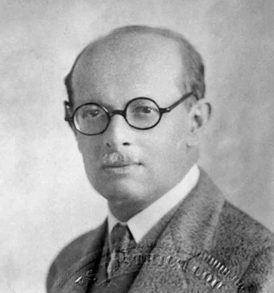
To start up with the invention story of transistors let us have a look on the people who were behind its invention. On October 22 1925 an Austrian-Hungarian physicist, Julius Edgar Lilienfeld recorded the first patent for transistors in Canada. But, as he did not make any research publications regarding the invention of the transistor, the industry ignored his work. Yet, he had a major role in the invention of the field effect transistor. Following the works of Julius, in 1934, a German physicist, Oscar Heil marked another patent for the field effect transistor. Though no findings were made at that time, later researches show that Julius Lilienfeld’s transistor gave a perfect result and gain. John Bardeen, William Shockley and Walter Brattain made parallel researches with germanium.
Julius Edgar Lilienfeld

 What was the necessity? 

Can you guess what made these people work so religiously on transistors? There is a role played by the germanium crystals behind the screen! The ultimate aim of the research was to produce a pure germanium crystal mixer diode that was used in the radars. These radars served the purpose of a frequency mixer.

The achievement with germanium

Purdue university proved success in producing pure and a standard high quality germanium semiconducting crystals. As tube based technology was not fast enough, they tried with solid state diodes. Learning more about this diode, they tried making out a triode; however, they found this process to be very tedious.
John Bardeen - Willian Shockley and Walter Brattain

Advancements with triode

John Bardeen developed surface physics which was an outcome of the research and the odd behavior of the previous study. Bardeen and Brattain succeeded in making a working device and then Shockley attempted to develop a triode based semiconductor device.

What is the base for invention?

The principle of transistor invention lies on understanding the electron mobility. If the flow of electrons from the emitter to the collector could be controlled by one way or the other, an amplifier could be built of the diode! It seemed very difficult, but Brattain made the move. When the team was working on building such a device, there were many flaws in the research.  At times the system worked and sometimes it unexpectedly stopped working.

And what can be the solution?

If there is a problem, there must be a solution. When a non working set up was placed on water, fortunately it started to work! Because of the net charges, the electrons in any one piece of the crystals would move. As opposite charges are more likely to attract, the electrons in the emitters and holes in collectors tend to move towards the surface of the crystal. The opposite charge was obtained from the air or from the water. These net charges can be easily pushed aside by the application of a very little amount of charge from some other portion of the crystal. A maximum injection of electrons that was needed to wash out the charges was then replaced with a minimal supply of the electrons. Thus, the researchers’ understanding paved way for solving the problem. There was no need of two separate or individual semi conductors; instead, a little larger single surface can be used as a replacement.

The new system

In the new invention, the emitter and the collector were located at the top which were close together and the control lead was placed on the crystal’s base. On applying current, the electrons or holes from the emitters and collectors were flushed out, across the semi conductor and they were collected at the far end of the crystal surface.

The first ever transistor

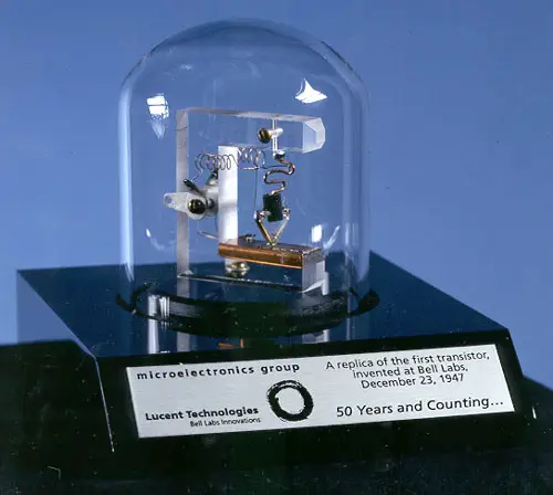
Replica of the first transistor made in Bell Laboratories - December 23 - 1947
Though there are many evolutions of the transistor, the first transistor was made after many failures. The BELL telephone laboratories tried on the process and faced no success. The invention of the point-contact transistor is another interesting story. It was found that when the contacts were more closely placed, the system or the set up became even more fragile. A gold coil was pasted at the end of a plastic wedge. It was then cut using a razor at the tip. It resulted in two closely placed gold pieces. It was found that current started to flow when voltage was applied on the other side of a crystal, after the plastic was pushed down on to the surface of that crystal. Thus the point contact transistor was invented.
It was on December 16 1947, the double point contact transistor was made, by creating a contact with germanium surface. This germanium was previously anodized to 90 volts and a few gold spots were evaporated. On pressing the gold spots against the bare surface, the gold was set to contact the surface perfectly.  The points were separated at a distance of about 4 X 10⁻³ cm. Among the two points, one was used as grid and the other was used as plate. Brattain and Moore demonstrated the set up to several of their colleagues and the invention of transistor was announced on 23rd December 1947.
John Bardeen, Walter Houser Brattain and William Bradford Shockley were awarded with the Nobel Prize in 1956 for this life-transforming research on semiconductors and their discovery (rather than invention) of the transistor.
Besides John Bardeen, Walter Houser Brattain and William Bradford Shockley, twelve more people are told to be directly involved in the invention of the transistors.

Transistron

In 1948, Herbert Matare and Heinrich Welker applied for patent on solid based transistors which were called as transistrons. Since there wasn’t any announcement from BELL, it was declared that transistrons were developed independently. These transistrons were commercially manufactured and was used in the French telephone Company.

 Credits

Vacuum Tube Invention History and Story behind Invention

Vacuum Tube Invention History and Story behind Invention

The story behind the invention of vacuum tube  

Anything in Science has its own history and some hidden truths behind its invention. It must be fascinatingly curious for any science savvy person to know the invention story of technical tools, and other innovations of Science. This is one such write up which will help you know about the researches and the advancements in the invention of the vacuum tubes.

Vacuum tube?

Vacuum tubes are sealed glass tubes made of vacuum that facilitates the passage of electric current. They are also called as electron tubes and they may be sealed either with glass or with a metal ceramic mixture. The application of this invention does not stop with a single one. They serve multiple purposes like amplifying a weak current, converting an alternative current (AC) to direct current (DC), for the generation of oscillating radio frequency.

The inventors!

If there is something awesome, it is true that great minds are involved in its invention. Professor Guthrie, Thomas Alva Edison, Ambrose Fleming, Lee de forest, William.D.Coolidge, Walter schottky and Irving Langmuir were those brilliant minds that were involved in the advancements of the electron tube.

The first leap! 

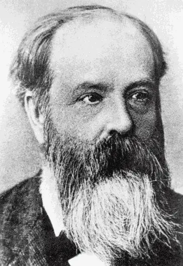
Professor Guthrie
Professor Guthrie - Copyright:- Wikimedia Foundation
It was Professor Guthrie who first worked with the unnamed vacuum tubes in the mid eighteenth century. He observed an effect, which showed, when a red hot iron sphere was negatively charged, it could discharge. But on the contrary, if the same hot sphere was positively charged, it did not get discharged! This remained as an unsolved puzzle until Edison made his move.

The solution for puzzle by Edison! 

Thomas Edison - Copyright:- Wikimedia Foundation
In 1883, Edison made an excellent move. When Edison was working with the incandescent lights and other bulbs, he faced a major problem. It was that the bulbs got blackened so quickly. Edison found that this was because the negatively charged particle hit the surface of the light bulb. He then made an alternative by placing positively charged particles. As we all know the fact that opposite charges attract each other. The negative charges were attracted by the newly introduced positive charges and thus it was prevented from hitting the surface of the bulb. He also found that when the second element was positive, then a current flow was occurring in the circuit. But, reversing the potentials averted this process. This was named as Edison effect and its purpose was unidentified. He discussed this effect with an electrical engineering professor from University College, London. He was Ambrose Fleming.

Further advancements in the discoveries 

John Ambrose Fleming:- Copyrght:- Wikimedia Commons
Only with the advancements by Professor Fleming, it was known that the atom had finest particles called electrons. And the reason for why it attracted the positively charged particles was identified by Sir Joseph Thomson. In 1889, when Fleming was working with the same Edison effect, he observed that when an alternative current was passed between 80 to 100 Hertz of frequency, only half of the cycle was completed. This was the observation that led to the above mentioned understanding that electrons were released from the heated filament.

The oscillation valve by Fleming

Marconi was working on wireless signals and was trying to increase the distance up to which they can be made to use. Fleming was working with Marconi. He observed that the sensitivity of the receiving tool was due to the detector’s lack of sensitivity. Coheres and magnetic detectors were employed which were of no better capacity and were not satisfying its purpose. When he was on a leisure walk in 1904, Fleming had a thought provoking and path breaking idea of applying the Edison’s effect in solving the difficulty. It was soon proved by his assistants that the idea worked. Since this involved a slow to and fro motion of electric waves, this was called as oscillation valve. This idea which was patented by Fleming was the major reason for a wireless technology in the future. Though there were still more advancements needed for the vacuum tube, it was far more superior to the magnetic detectors and the coherers. In spite of all its advantages, the vacuum tubes experienced pit falls. It required a large amount of power, which was to be supplied by highly expensive batteries. To overcome these disadvantages, relatively cheaper devices were invented later. Two different patents were filed for the devices. The first patent was for Ferdinand Braun for a manganese oxide hydrated crystal and the other patent was for a carborundum crystal by H.Dunwoody.

The highly advanced vacuum tube 

Lee De Forest - Copyright:- Wikimedia Commons
With all the advancements and the advantages of the newly developed crystal detectors, people craved behind the vacuum tubes. The most crucial step for the development of vacuum tube was made by Lee de forest. His notable remark was that he held more than 300 patents. He worked on a wide range of wireless technologies. His father was a congregational minister. He was not supported by his parents. The invention of audion tube was his most known invention. The audion tube consisted of triple elements and its uniqueness was that the current was controlled by a grid. This was the invention that paved way for the radio. He initially worked on Fleming’s diode valve and then introduced a third electrode into it. In this three electrode device, the new electrode was placed between the anode and the cathode. This was supported by a grid like structure. Only by 1911, the vacuum tube was first used as an amplifier. Professor Lee de forest demonstrated a new idea to the telephone company, A.T & T. His new idea was building an amplifier by employing three audions. When he demonstrated, the efficiency was poor, but since they realized the potential of this, they adapted the experiment and made further advancements to rectify any blunders. Once the vacuum tube was used as an amplifier, people started to using it as an oscillator as well. But, soon the problem was in preventing oscillations in regard to the high value of the grid anode capacitance.
So that’s all about the story behind invention of vacuum tubes. We hope you have enjoyed the story and in the process gained really valuable insights and information as well. Wait for other stories in the series!

Solar Cell – Invention History & Story – From Selenium to Silicon

Solar Cell – Invention History & Story – From Selenium to Silicon

Invention History of Solar Cells – From Selenium to Silicon

Well, the definition of a solar cell is simple. It is a device that directly converts the energy from sunlight into electrical energy. However, its horizons are really vast. The most significant fact is that the invention of this wonderful device didn’t happen overnight. Interestingly, the concept of solar technology is nearly three millenniums old. The first use of this wonderful technology dates back to 7th Century BC.
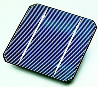
Solar Cell - Invention History & Story.
Solar Cell - made from Silicon wafer (Source:- Wikimedia Commons)

First Recorded Utilization of Solar technology

A magnifying glass was used to concentrate the sun’s rays to make fire. And would you like to know what the purpose of making this fire was? You may never guess it right….It was to burn ants!!! Now, that proves the saying ‘Necessity is the mother of invention.’ So, this was how man started using this massive energy source to serve, perhaps, a trivial purpose. Since then, scientists and innovators have made a lot of attempts to make use of this immense energy from the sun in various walks of life. In fact, many succeeded in inventing quite a few useful devices as well.

Notable development of solar cell technology

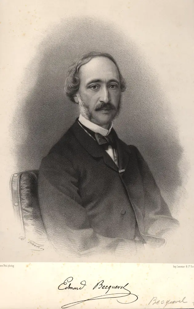
It was the research of the French physicist Edmund Becquerel that set a milestone in the development of the solar cell technology. This historical highlight occurred in the year 1939 when Becquerel was just 19 years old. One day, when he was working on an experiment with an electrolytic cell, he reported of the photo voltaic effect for the first time. The electrolytic cell was made up of two metal electrodes. When Becquerel placed this cell in an electrolytic solution and exposed it to a little light, he noticed the photo voltaic effect. He also noticed that as the light intensity increased, the photovoltaic effect or electrical current also increased. So, this was an early breakthrough in the invention of a solar cell.
Invention History of Solar Cell
Edmond Becquerel - French Physicist (Source:- Wikimedia Commons)

Photovoltaic Effect and Selenium Cell

It is really amusing to know how selenium came to be linked with Photovoltaic effect. This incident happened sometime in the 1860s. Willoughby Smith, an electrical engineer, was testing underwater telegraph lines for any faults. He was using selenium for this purpose. While he was sincerely doing his work, he happened to notice a strange effect: When selenium was exposed to light, electricity traveled well through it whereas it failed to do so when selenium was kept in darkness. Therefore, it was Smith who accidentally discovered that electricity could pass through selenium very well.
Later, in 1876, W.G. Adams and R.E. Day worked on this aspect and observed the same effect in solidified selenium. They proved that sun’s energy does create a flow of electricity in selenium. Besides, they also published a paper on the selenium cell. Following these two, several scientists worked on this to understand more about selenium and photovoltaic effect.

Now, who managed to build the first photovoltaic cell?

It was the American inventor Charles Fritts who built the first genuine solar cell. He built it by placing a layer of selenium on a metal plate and covering it with a thin layer of gold. Though this cell had only about 1% efficiency, it was a good start and proved to be helpful in the development of early light sensors used in the cameras.
Though a couple of scientists were curious about this invention, most scientists paid little attention. Having known that only black materials capture the sun’s heat energy, they were not able to figure out how a cell that wasn’t black in color used sun’s light to produce electricity! Perhaps, so little was their knowledge on solar energy.
In those times, since there were better technologies to generate electricity, the PV technology failed to attract the masses. In fact, in modern terms, it was a flop.

The Comeback

It was Albert Einstein who made a major breakthrough in the development of solar technology.He set his mind to understand how light could possibly create electricity when it hit a metal. Einstein knocked down everyone with his terrific explanation. He explained that light was made of tiny packets of energy called photons. He also elaborated on how photons wiggled like waves as they sped along. Einstein proposed that these photons are more powerful in ultraviolet light that in the normal light that we can see. He also added that these photons have enough energy to knock the loose electrons off some materials like silicon and selenium. These knocked out free electrons move through wires as electric current or electricity.
After testing these ideas, many scientists were convinced. It was for these ideas that Einstein won a Nobel Prize. So, all the credit goes to Einstein who paved a path for the future scientists who made more efficient photovoltaic or PV cells.

Cheap oil and gas win over solar energy

In the late 1800s until the 1920s, oil and gas were cheaper options of generating electricity. So during this period, there wasn’t much interest shown in solar energy. However, a few scientists did not lose hope and kept trying their best to find a way to use solar energy to generate electricity.

Various issues with photovoltaic cells

In 1931, a German scientist named Bruno Lange succeeding in building a solar panel out of selenium. Unfortunately, Lange also faced the same problems as Fritts. The amount of electricity generated through this solar panel was too low and hence it was not very useful. Besides, the selenium cells also failed to last long in intense sunlight. These drawbacks made experts feel that PV cells cannot serve as a good way to produce electricity. The next ten years, the concept was almost buried.
However, in the 1940s, people again became interested in solar electricity generation.

Use of Silicon – A breakthrough

It was in the 1950s that the idea thrust up with full force, and this time, in a different and successful way. In the early 1950s, Calvin Fuller and Gerald Pearson were working on improving silicon transistors for electrical devices at the Bell Laboratories, USA. Accidentally, they created a PV cell that produced electricity when placed in light. The cell they created was made of two different types of silicon that had dissimilar metals mixed in.
During the same period of time, another Bell scientist Daryl Chapin was trying to make developments in employing selenium cells to generate electricity. Well, he wasn’t that successful in his efforts. Then, one fine day, Pearson happened to discuss his accidental silicon PV cell with Chapin. Chapin became really excited and started looking into it straight away.

The ultimate discovery of efficient silicon solar cells

The Bell scientists were amused at the new idea that silicon PV cells were capable of producing five times more electricity than the selenium PV cells. The three of them spent one complete year experimenting with the silicon cells in order to make sufficient electricity to make these cells really useful. At last, after facing a lot of disappointments, they made their way to success. They achieved it by mixing small amounts of different chemicals into silicon crystal slices. This silicon solar cell they invented was able to directly convert sunlight into enough electricity to run electrical equipment. These silicon solar cells were about 50 times more effective than the selenium cells discovered two decades earlier. Thus, the silicon solar cells came to exist.

Shockley Diode – Invention History

Shockley Diode – Invention History

What is a Schockley Diode?
In simple terms, a Shockley diode is a four layered semiconductor diode. In electronic terms, it is a “P-N-P-N” diode and is equivalent to a thyristor with a disconnected gate. Though this basic diode does not find much application in electronic circuits nowadays, the concept is largely employed and is one of the remarkable inventions in the history of electronics.
The interesting history of the Shockley diode cannot be interpreted without mentioning a few important life events of its inventor, the popular physicist and the co-inventor of the transistor, William Bradford Shockley.
To know more on the working, characteristics, and applications of Schockley Diode go through the link - Schockley Diode

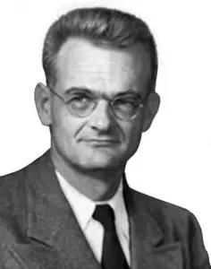
William Shockley: Experience at Bell Labs

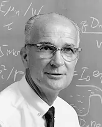
William B Schockley
William B. Shockley
William Shockley was an American engineer and professor who was brought up in Palo Alto, California. He did his under graduation in Caltech and completed his PhD in MIT. After graduating in 1936, he chose to start working at Bell Labs. For about two decades, he worked on electronic devices and more on semiconductor materials. His research paved way for the creation of the first transistor in 1947 along with Walter Brattain and John Bardeen.
After the invention of the transistor, Shockley noticed that Bell’s management was promoting Bardeen and Brattain’s names ahead of his on the patent of the transistor. But, some of his colleagues were of the opinion that these issues were the result of the abrasive management style of Shockley. Such unfavorable events in the early 1950s made Shockley really upset with the management of Bell Labs. These issues were at its worst in 1953, causing a cut throat situation for Shockley and he made the most remarkable and stern decision of his lifetime to quit Bell Labs and he returned to Caltech as a visiting professor.
Return to California – Foundation of Shockley Semiconductor Laboratory
At Caltech, Shockley became friends with Arnold Orville Beckman, the inventor of the pH meter. It was then that Shockley learned more about the inherent capabilities of silicon and was convinced that silicon would certainly and ultimately replace germanium as the primary material used for transistor construction. It was during that time, that is, in 1954 that Texas Instruments had started manufacturing silicon transistors. Shockley believed that he could do something more in this arena. Beckman backed Shockley’s efforts and belief under the umbrella of his Beckman Instruments.
In September 1955, Shockley and Beckman co-founded the Shockley Semiconductor Laboratory in Mountain View, California as a division of Beckman Instruments. The division was primarily found to engage promptly, vigorously and exclusively in research related to semiconductors. Shockley rented a building at 391 South San Antonio Road in Mountain View for this purpose. The site is now home to a furniture store and its sidewalk bears a commemorative inscription stating: “At this location in 1956, Dr. William Shockley started the first silicon device research and manufacturing company in the valley.”
Shockley recruited the most creative and intelligent team of young scientists and engineers in the world for developing and manufacturing transistors, mainly single-crystal silicon boules. At that time, producing such silicon products was a difficult prospect because of the high melting point of silicon.

The invention of the Shockley diode – The first step towards the formation of the Silicon Valley

While the research on the silicon transistors continued, all on a sudden, Shockley hit upon the brilliant idea of using a four-layer device (a transistor is a three-layer device) that would possess the unique and novel quality of locking into the “on” and “off” state without any further control inputs!! Such circuits normally required about three transistors; therefore, he thought that the new diodes can greatly reduce complexity for large switching networks. This four-layer diode was later named as the Shockley diode.
Shockley was convinced that the new device was just as significant as the transistor and he maintained the entire project as a top secret, drawing an ‘iron curtain’ even within the company. This led to his paranoid behaviour increasing day after day. He was also becoming indecisive most of the times; sometimes he thought that starting immediate production of the basic transistors was important; sometimes he stressed on the Shockley diode project. This really upset most of his employees and frequent rebellions became common within the company. Ultimately, a group of eight youngest employees complained to Beckman demanding replacement of Shockley in the management role.
Later, these eight left Shockley’s Semiconductor Laboratory to form a different company and gradually each one started founding new companies. Thus, Shockley’s attempts to commercialize the new four layer diode led to California’s “Silicon Valley” which is now the hotbed of electronics innovation.

Shockley’s diode – A commercial failure

Unfortunately for Shockley, he was never able to make the four-layer diode a commercial hit despite working out the technical details and entering production in the 1960s. The invention of the integrated circuits allowed multiple transistors required to produce a switch to be placed on a single chip. This invention, eventually, nullified the parts-count advantage of Shockley’s four layer diode design. On the other hand, the four layer diode was, in essence, the first integrated circuit because it performed the work of two transistors, two resistors and a diode, all in a single crystal. Unluckily, making these devices was a tricky task; so, Shockley could never manage to build truly commercially viable ones.

 Significance of Shockley diode

The four-layer diode was the key to Shockley’s plan of revolutionizing the phone system of AT&T. It was indeed a great device in theory, but not in practice. The Shockley diode is a crystal made of alternating layers of N-type and P-type semiconductors. Having four layers, the Shockley diode perhaps could do more than a transistor. Besides, it could act like a rectifier, turning alternating current to direct current. Moreover, when break-over voltage was applied, it could switch on and off. Thus, these diodes could be used to replace rectifiers and transistors required to connect long distance phone calls.
Four-layered semiconductors are used today in the form of thyristors and thus, Shockley diodes do exist.
What could explain the revolutionary idea behind the Shockley diode better than these words of Harry Sello?
“It was to be used in telephone exchanges and Shockley felt it would be revolutionary product that would replace all the mechanical relays in these gigantic electronic switching stations and it would revolutionize the industry. And the idea was true. The trouble with the four-layer diode was it was three years ahead of its time in processing complexity and we just couldn’t make it.”
Sello sums it up!!!

Zener Diode – Invention History & Story Behind the Development

Zener Diode – Invention History & Story Behind the Development

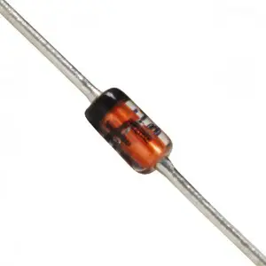
Zener Diode
Zener Diode
As we all know, a Zener Diode is used for regulating voltage in practical circuit applications. Though we know about the importance of this device, do we really mind knowing about how it was invented? If you had that query in your mind, then reading further would give you a thorough knowledge on the discovery of Zener Diode and its properties. You shall also be informed of the great scientists who worked on this device. Before going into the invention story, let us have a brief note on what a Zener Diode is.

Zener Diode

This semi-conductor device permits the flow of current in a unidirectional way. Provided with sufficient voltage, they allow the flow of current in the opposite direction as well. The excess voltage required for reversing the direction of flow of current is termed as breakdown voltage or Zener voltage. The major role of a Zener Diode is to function as a voltage regulator. It is fairly employed in many electrical and electronic tools and equipments. The Zener Diode varies in a wider range based on its mounting location. Most of them are either mounted onto a surface or found in holed components. The surface mount Zener Diodes are directly mounted on a printed circuit board. In the other technique, components are attached to the holes with the help of wires. The codes that represent Zener Diodes always begin with either of the letters BZX or BZY.

The early history of Zener Diode

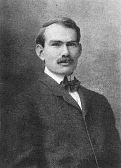
Clarence Melvin Zener
Clarence Melvin Zener - Inventor of Zener Diode
Only when the need for semi conductor materials exceeded, the urge to develop a device like Zener Diode spread deeper and wider. Many early inventions were made till 1905, yet a more focused work on semiconductor devices were started only at the time of the Second World War. It was Clarence Melvin Zener who first elaborated on the advantageous properties of this diode.

Clarence Melvin Zener 

Clarence Zener was a professor at Carnegie Mellon University in the department of Physics. His interests were focused on solid-state physics. In 1926, he graduated from Stanford University and received his doctorate from the Stanford University by 1929. He developed the Zener Diode in 1950 and employed it in modern computer circuits. Clarence Zener published a paper on explaining the electrical insulator’s breakdown in 1934.
He was recognized across the world for introducing a field of science with internal friction which was the subject on what most of his studies were focused.

Principle behind the invention of the Diode

The very basic principle that paved way for invention is the unidirectional way of flow of current. The very first Diode by Sir Thomas Alva Edison was a light bulb with certain modifications on it. Edison noticed that with an additional electrode, and connection to the positive side, facilitated the current flow from the filament towards the empty space.Though he observed, Edison was not at all sure about the physics behind this effect.Joseph J Thompson explained the reason behind this and was awarded the Nobel Prize in 1897. This lead to the invention of vacuum tube diodes. You can read the incredible story behind invention of Vacuum Tubes to know more about the people behind.

Pre- Zener Diodes

Many other scientists were interested in finding the alternative usage of this principle. John Ambrose Fleming tried using this valve for converting radio waves into signals that could be measured by employing a galvanometer. The Fleming valve is recognized to be the first true electronic device as of now.
In 1906, Greenleaf W. Pickard invented another new Diode. With his earlier studies, Pickard confessed that electrons can flow only in a single direction, employing certain minerals like silicon. Placing a silicon piece between a metal base and a metal wire, he developed a valve that can be utilized in detecting the radio waves.
This was named as cat’s whisker Diode as fine wires were employed in it. H. C. Dunwoody patented a developed form of this Diode that had the employment of carborundum in it.

Limitations of Cat’s whisker Diode

Though they were a revised version of electron tubes, they had certain limitation that shortened its usage. The first limitation was that they were more fragile and were prone to misalignment. Hence they required a very careful adjustment. Considering this reason, the use of cat’s whisper Diodes were fairly reduced, neglecting its advantage of working even in a very high frequency.
During the period of the Second World War, the BELL laboratories developed another new type of diode usingsemiconductors (silicon & germanium). Russel Ohl, who was a metallurgist in the Bell laboratories, developed a diode using Germanium crystal that produced electricity in response to light. It was facilitating the conversion of solar energy to electricity.  It was found that the silicon piece that was cut has a large amount of impurity. The area where the impurity joined the silicon was termed as the junction. Years later, it was found that the impurities had developed response to the solar particles. This lead to invention of semiconductor based PN junction diodes. You can read the amazing story & series of events occurred at BELL labs during the invention of PN juction diode to gain more knowledge. Even before the identification of the reason, the production of these solar converters hadbeen initiated.
The usage of Diodes thus slowly expanded from time to time. Electron tube diodes are used very rarely. But then, the diodes that are made out of the material silicon have a wider application. This helps in detecting the high frequency electromagnetic waves. They also serve as components for the conversion of energy obtained from Sun to electrical signals. Inside many electronic devices like televisions and the computers, the diode systems are employed for averting the alternative current (AC) to direct current (DC) and also in the regulation of the voltage level.
Automobiles are imparted with high potential Diodes. Their role is also similar to that of the other Diodes like converting the AC to the DC. In the early 1906, incandescent lamps were replaced with the LED or the light emitting Diodes. The lights used in the headlights of car and other light bulbs are also very likely to be replaced with the light emitting Diodes.

Radio-Invention History & The Story of Fight for Patents

Radio-Invention History & The Story of Fight for Patents

Radio – Invention History

The invention history of the radio is not only interesting but rather long as well. If you ask who invented the radio, probably you will get the name Marconi. But, was it really Marconi who invented the radio? Well, you have to determine for yourself after going through the journey of the invention history of the radio.
There are a lot of knots to be untangled if you want to arrive at an answer as to who invented the radio. Was the inventor of radio the person who discovered that electromagnetic waves can be sent through air? Was it the person who sent signals to the farthest distance? Was it the person who sent the first signals with voice? Well, the answers are in fact not easy.
Wireless itself is relatively a broad concept. Within the wireless category itself, there are many subcategories of which radio broadcasting is just one; the others include wireless telegraph, wireless ship-to-shore communication, and the like. To know the development of wireless, it is crucial to first track the events that led to the discovery of electricity. Though there is early documentation, it was in 1600 that electricity as a science had its beginning. It began when Dr. William Gilbert, Queen Elizabeth’s personal physician invented the electroscope which could detect electromagnetic energy in the human body. Gilbert coined the word ‘electricity.’ From there, a lot of researchers and scientists had their hand in the development of this wonderful field of science. Sir Thomas Browne, Alessandro Volta, Benjamin Franklin, and Georg Simon Ohm were a few among the many who made several contributions to the science of electricity.
Radio is, in fact, indebted to other major discoveries for its birth: the telephone and the telegraph. Perhaps, these three technologies are very closely related. Radio first started as wireless telegraphy. And, the credit certainly goes to the invention of the radio waves which was found to be capable of sending out music, speech, picture and various other data through air.

Exploring Wireless

The true interest in wireless began with the invention of the telegraph in 1837 by Samuel F. Morse in 1937; the telegraph required wires which was a bit expensive proposition during those times. In the 1860s, James Clerk Maxwell, a Scottish mathematician and physicist, was the first to forecast the presence of radio waves; however, he was not able to prove his theory. Following him, several researchers tried various means to showcase the presence of the radio waves. But, the real experiments that led to the discovery of the Radio started with Heinrich Hertz in 1887. A few call him the father of Radio because it is known that his experiments instilled interest in Marconi. In those days, Radio waves were called Hertzian waves.  Hertz showed the projection of swift variation of the electric current into space in the form of radio waves. Hertz then measured the velocity of the waves and found they were the same as light, 186,000 miles per second.

Tesla and Marconi

When the world was heading towards the 20th century, inventors all over were trying on new and exciting inventions. A lot of scientific work in radio technology was heating up as well. In the race to invent the radio, two men, a Serbian-American scientist Nikola Tesla and an Italian physicist Guglielmo Marconi went head to head. However, even today or a hundred years later, ask any two people about who invented the radio and I bet you – you will probably get two different answers. The story is perhaps a foggy one that is a mixture of scientific discovery with lawsuits and some old-fashioned marketing.

Tesla’s Part
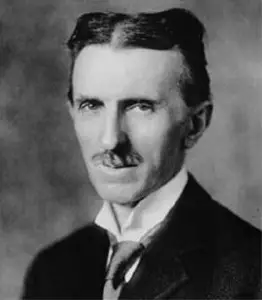
Nikola Tesla
Nikola Tesla – Founder of Tesla Coil
Tesla invented the induction coil or the Tesla coil after he came to the US in the year 1884. A Tesla coil is a device required to send and receive radio waves (it is said that Marconi relied on this coil for his experiments). In about 1895, unfortunately, Tesla’s laboratory was completely destroyed by fire when he was preparing to send a radio signal about 50 miles to the West Point, New York.

  Marconi’s Research and Invention 
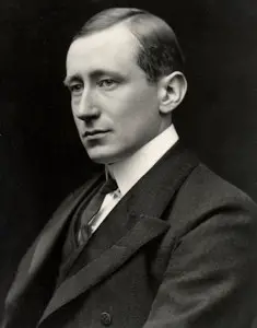
Guglielmo Marconi - Wireless Telegraphy
Guglielmo Marconi – Wireless Telegraph
Twenty years after the telephone was invented, music was set down on telephone line and Marconi was the one responsible for the radio signals. The Italian discoverer showcased radio communication’s feasibility. He was fascinated by Hertz’s discovery of the radio waves that he realized it could be employed for receiving and sending telegraph messages; he referred to it as wireless telegraphs. Marconi’s earliest radio transmissions transmitted coded signals to only a mile far in the year 1896. Later Marconi recognized the huge potential of these waves and offered the discovery to the Italian government. Unluckily, the government turned it down. Marconi then realized a patent and started experimenting further after he moved to England. In 1896, Marconi sent and received Morse code-based radio signals at distances spanning approximately four miles. The same year, he applied for and was granted the world’s first patent in wireless telegraphy. It was in England that he received the first patent. In 1898, he made the first ever public broadcast of a sports event – he flashed the results of Kingstown Regatta to Dublin Newspaper office.

The Fight for Patents

Tesla applied for his first patents for his radio work in 1897 in the US. He also constructed and demonstrated a radio-controlled boat at the Madison Square Garden in the year 1898. And, this was where things started getting sticky.
In 1900, the US Patent Office granted Tesla with patents for the fundamental design of the Tesla coil. The radio patents offered to Tesla gave him the ownership over one of the major necessities in radio communications. Towards the end of the same year, Marconi filed a patent for tuned telegraphy. The patent office first denied Marconi’s applications saying that his work relied on the use of Tesla coils. Not getting discouraged, Marconi made use of his father’s contacts and wealth to lead a lucrative business based on his telegraph technology; meanwhile, he continued to pursue his radio patents. In the year 1901, he transmitted the first transatlantic telegraph. Marconi continuously applied for the patent for three years while he also gained financial support from company investors like Thomas Edison and Andrew Carnegie. Finally, in 1904, the US Patent Office strangely reversed its earlier decision and gave Marconi the patent for the invention of the radio. Marconi also won the Nobel Prize for physics in 1909. This further fueled the rivalry with Tesla.
After a lot of lawsuits, the US Supreme Court restored Tesla (who had died a few months earlier) as the inventor of radio!! However, many people still believe that Marconi is the father of the radio.

Another claim by JC Bose
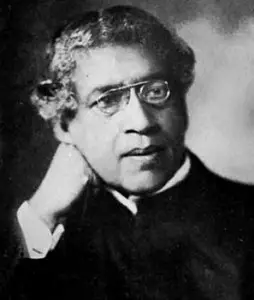
J C Bose
J C Bose
JC Bose of India was another claimant to the throne of radio inventors. In 1896, he demonstrated radio transmission to the British Governor General at Calcutta in India. The transmission covered a distance of around 3 miles. The instrument he used, the Mercury Coherer attached to a telephone detector, is still displayed at the Calcutta University’s Science College. Bose had overcome Hertz’s problem of waves not being able to penetrate through mountains, walls or water. Marconi’s Coherer and Bose’s Coherer were exactly the same. Bose was hesitant about applying for a patent because he was a firm believer of free flow of inventions in the field of science. However, due to the persuasion of his American friends, he had applied for a patent in 1901. In the year 1904, the US patent was granted to him.

Nathan Stubblefield – A Significant Personality                
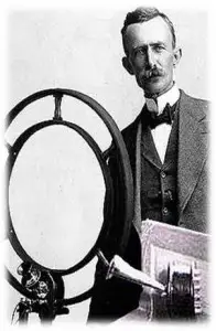
Nathan Stubblefield
Nathan Stubblefield
Even before Tesla and Marconi made their way towards the Radio, Nathan Stubblefield, a Kentucky farmer and inventor, demonstrated wireless technology in public in the year 1892. He was able to broadcast signals as well as voice and music!! In 1898, again he demonstrated wireless to a documented distance of about 500 yards. Later in 1902, he showcased a ship-to-shore broadcast on the river Potomac in Washington DC; for this, he received a patent for wireless telephone in 1908. Stubblefield was actually afraid that someone would steal his idea and invention that he tried every possible means to shelter it from everyone. Once he was offered $500,000 for this invention but he refused as thought his invention deserved more. He envisioned the device in motorcars. Following a demonstration in Washington in 1912, his whole device was stolen. He firmly believed that his invention was copied. Sadly, Stubblefield died of starvation after going into seclusion because of his failed attempts for acceptance of his invention.
Now, who is the actual inventor of the Radio?
Well informed professionals still feel that the whole credit of the invention of the radio should go to Stubblefield. If you visit the Town Square in Murray, Kentucky, you can find a statue of Stubblefield with an inscription “Murray, Kentucky, Birthplace of Radio.” Now, who is the inventor of Radio? The US Supreme Court ruled that Tesla is the father of Radio and Marconi is not. The question still remains whether the honor should really go to Stubblefield or rather Bose.

Evolution of the Radio

Radio has evolved tremendously over the years. Earlier, transmitters were called spark gap machines. They were mainly established for ship-to-ship and ship-to-shore communication. Those days, communication was limited to two points and did not involve public broadcasting as it is today. In case of sea disasters, wireless signals displayed effective communication for rescue operations. A range of ocean liners started installing the wireless equipments and in 1899, the US Army set up the wireless communication. Two years later, the Navy adopted the wireless system; it was a great relief because until then, Navy was using homing pigeons and visual signaling for communication.
In 1901, radiotelegraph services were established in the Hawaiian Islands. Marconi station located in the Massachusetts carried greetings between Theodore Roosevelt and King Edward VII. In the year 1905, Port Arthur’s naval battle was reported of using wireless communication and the US weather department used radiotelegraphy.
Sooner, radio transmitters were improved a lot. Overseas radiotelegraph services slowly started developing. Lee Deforest, the inventor of space telegraphy, Audion, and triode amplifier, took care of the developments in many technical issues. Deforest also discovered the detector. In fact, he was the first person to use the term ‘radio.’ His work resulted in the discovery of AM radio that was capable of broadcasting several radio stations which the earlier gap transmitters did not allow.
Ever since that time, there has been no looking back. The radio has now become a popular medium of handy entertainment. With the technological advancements in the 21st century, the Internet radio is also introduced. Satellite radio is another recent development in the field. Using this, one can listen to several international radio stations without any issues. In addition to all these latest editions, Ham radio is the next big thing. No wonder radio lovers have a reason to celebrate as there is perhaps a lot in store for them!!